Ultiboard Tutorials

Best Practices for Printed Circuit Board Routing

Overview With the integrated capture, simulation and layout environment of the National Instruments Circuit Design Suite, engineers have a complete…

Overview

With the integrated capture, simulation and layout environment of the National Instruments Circuit Design Suite, engineers have a complete PCB design and validation environment. With the integration with NI LabVIEW, measurements can be easily introduced into the design flow, with simulation results improved with real-world data (a concept called virtual prototyping), and the transfer of simulation data to the test environment to compare real vs. theoretical. 

In this series of Best Practices articles, National Instruments provide a number of new resources to show you how to use various features in NI Multisim and NI Ultiboard in the most advantageous way to save time and maximize resources.

Table of Contents

  1. Introduction
  2. Routing of Copper Traces
  3. Getting Started
  4. Method 1 Manual Trace Placement
  5. Method 2 Follow-Me Router
  6. Method 3 Connection Machine
  7. Method 4 Autorouter
  8. Best Practices: Maximizing the Use of Your Routing Methods

1. Introduction

In this introductory article we will investigate the various techniques available for copper routing in NI Ultiboard, how to use them, and when to use them.

Back to Top

2. Routing of Copper Traces

In Printed Circuit Board (PCB) design, there are three fundamental tasks that allow you to prepare a board for prototype and manufacture. First the board outline must be created for the form factor of the design.

Second in consideration is part placement. In part placement various landpatterns (or footprints) of design devices are configured on the board. Each placed part consists of pins which are terminals that need to be connected in order to complete the design. A PCB design tool represents the necessary connections between parts with a wire. These wires are called nets. 

Therefore the third fundamental task in board design is to route these net connections between various parts. The routing processturns these various net connections into copper traces which connect parts in the physical prototype with current carrying connections. The net acts as a design guide indicating that two pins must be connected, while the copper trace is the actual physical connection which will be made as a part of your PCB.

NI Ultiboard allows you to define copper traces using a number of different methods. Each method provides varying degrees of control that allow an engineer to balance precise copper definition with automated speeds in order to effectively design a PCB. The routing methods available to engineers are:

  1. Manual Trace Placement
  2. Follow-Me Router
  3. Connection Machine
  4. Autorouter

In this article we will investigate how and when to use each of these routing methods.

Back to Top

3. Getting Started

To assist in the steps outlined in this article, we will use the attached example file to practice routing.

  1. Download the attached 6880_Example_Design.ewprj (Right click "Save File As") file to your desktop.
  2. Select Start > All Programs > National Instruments > Circuit Design Suite 10.0 > Ultiboard to open Ultiboard.
  3. Select File > Open.
  4. Browse to the desktop where you saved 6880_Example_Design.ewprj.
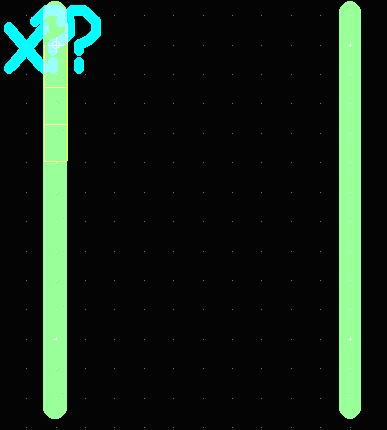
  5. Click on the Open button to view the file (as seen in Figure 1 below).

6880 figure 1

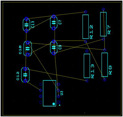
Figure 1: 6880_Example_Design.ewprj

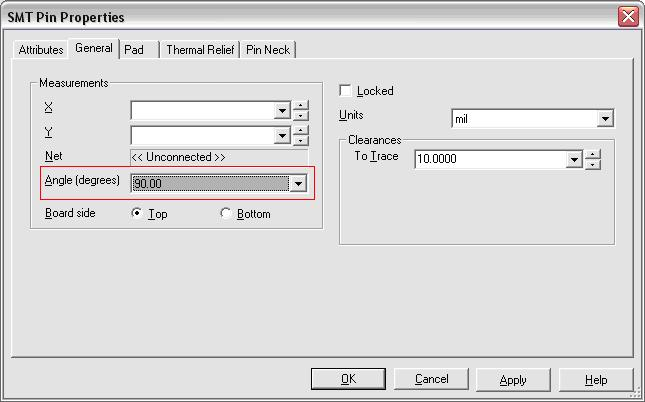
Follow the next steps to ensure that your work area is correctly setup:

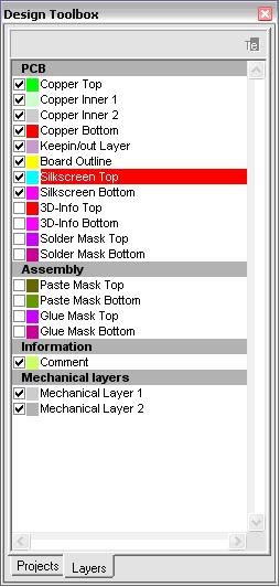
  1. Notice that on the left side of the NI Ultiboard screen you have the Design Toolbox (if you cannot see this currently you can view it by selecting View > Design Toolbox).
  2. On the bottom of the Design Toolbox select the Layers tab.

Whenever you are placing copper routes in the work-area you must first select the layer upon which the route will be defined. In this example we will be using the Copper Top however any of the copper layers (Top, Bottom, Inner) can be selected in the Design Toolbox.

  1. Double click on the Copper Top layer in the Layers tab (it will now be highlighted in red as seen in Figure 2 below). You are now ready to draw routes upon the top copper layer.

6880 figure 2

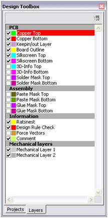
Figure 2- Design Toolbox

Back to Top

4. Method 1 Manual Trace Placement

What is Manual Trace Placement?

Placing traces with the line drawing tool allows the user to completely control every aspect of a copper trace. This drawing tool follows your mouse cursor and creates a copper route according to your exact specifications.

Other than following your mouse it is important to note that since you have complete design control you must be careful not to create routes that will cause design rule errors or put into questions the validity of your design. This means that sharp or obtuse angles in your routes should be avoided that will cause you to lose signal integrity.

When to use Manual Trace Placement

The manual trace placement is recommended when you have a part that requires a very specific routing, particularly when you have a surface mounted connector (with a high pin count), FPGA or very restrictive spacing between adjacent pins, the manual trace tool will give you the needed accuracy to properly define your route. Other methods such as the autorouter (discussed later in this article) may not be able to mathematically define how to route suitably in these situations.

How to use Manual Trace Placement

In this example we will make a manual connection between part C13 and part R12. To use the manual trace placement tool:

  1. In Ultiboard select Place > Line.
  2. With the mouse left-click once on the top pin of part C13 (figure 3 below)

6880 figure 3

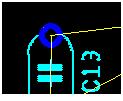
Figure 3 - Component C13

  1. As you move the mouse away from the pin you will notice a neon-green connection trail your movement. Move your mouse in the direction of the net connection between C13 and R12.
  2. To place a pivot point for your copper route, left-click with your mouse anywhere in the black work-area of your design. You have now defined the placement of this segment of your design (as seen in Figure 4)

6880 figure 4

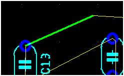
Figure 4 - First routed segment

To create an orthogonal section to a copper route, you can simply click on the SPACE BAR on your keyboard, and Ultiboard will automatically create a route that is exactly 90 degrees to your mouse movement. Click on SPACE BAR again to exit orthogonal mode.

  1. Complete the route and connect C13 to R12 as seen below in figure 5, by using the SPACE BAR to create the orthogonal route.

6880 figure 5

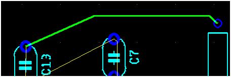
Figure 5 - Manual Trace Placement Routing

Back to Top

5. Method 2 Follow-Me Router

What is the Follow-Me Router?

The follow-me router adds to the functionality of the manual trace placement tool, with Ultiboard beginning to make some design decisions on your behalf. With the follow-me router, your mouse again defines the shape of the route however Ultiboard will automatically suggest pivot points and the route between two pins, with a light blue trace connection. Also if your route must be narrowed at all to make the connection appropriate (to get between pins etc…), Ultiboard will automatically narrow your route.


When to use the Follow-Me Router

The follow-me router is an appropriate tool when you need some guidance on how to connect two components but still want to be able to define the route, pivot points etc… Generally if you do not need precision of manual placement, but would like assistance in creating traces which do not conflict with good design practices (sharp angles etc…) then the follow-me router is an appropriate tool. It would still be recommended to use manual trace placement for high pin density chips and FPGAs.

How to use the Follow-Me Router

In this example we will make a follow me router connection between part C13 and part C7. To use the follow-me router placement tool:

  1. In Ultiboard select Place > Follow-Me.
  2. With the mouse left-click once on the bottom pin of part C13.
  3. Notice that as you move the mouse a light-blue connection guide appears between the two pins (figure 6). This is an Ultiboard suggestion for routing.

6880 figure 6

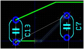
Figure 6 - Ultiboard Trace Guide

  1. Continue to move the mouse towards the pin of C7 and notice that pivot points are automatically placed in your design.
  2. To add your own pivot points, simply left-click once anywhere in your design.
  3. Complete your connection between C13 and C7 (figure 6)

6880 figure 7

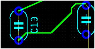
Figure 7 - Completed Follow-Me Route

Back to Top

6. Method 3 Connection Machine

What is the Connection Machine?

Again we continue to build upon our more manual processes (manual trace placement, follow-me router) with the Connection Machine. The Connection Machine can be considered to be a subset of the autorouter. The connection machine automatically defines a route, but does so, on a net-by-net basis, with a minimal amount of user intervention to customize the route.


When to use the Connection Machine

The connection machine is not for components with a high number of pins, or with a need for a complex routing arrangement.  As we move to the connection machine generally a larger amount of space is required with less need for precise routing.

How to use the Connection Machine

In this example we will make a connection machine route between part C10 and part C9. To use the connection machine tool:

  1. In Ultiboard select Place > Connection Machine.
  2. With the mouse left-click once on the bottom pin of part C10.
  3. Move your mouse slightly and notice that two small white crosses appear at the bottom pin of C10 and top pin of C9 (highlighted in red in figure 8 below).

6880 figure 8

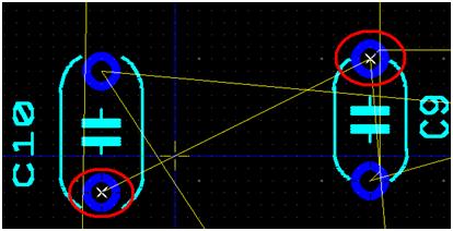
Figure 8 - Connection Machine Selection

These white crosses indicate that these are the pins to be routed together by the connection machine.

  1. Move the mouse slightly to the left of C10 (maintaining the two small white crosses) and click on the black work area between the two points. Two larger white crosses will appear between the two pins to be routed (highlighted in red in figure 9 below).

6880 figure 9

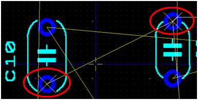
Figure 9 - Connection Machine Selection Validated

  1. Move the mouse cursor up and down and notice that the route is created automatically between the two points, with the movement of the mouse defining the route.
  2. Left-click once more to settle on a route configuration (as seen in Figure 10).

6880 figure 10

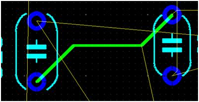
Figure 10 - Connection Machine Defined Route


Back to Top

7. Method 4 Autorouter

What is the Autorouter?

The autorouter can potentially be the fastest way in which to configure the routing of all the copper on your board. The router goes through a number of steps, most notably:

  • Determining the approximate direction and route of each net on a board
  • Selecting a sequence in which the nets are to be routed
  • Routing each net in the sequence previously determined

If the routing cannot be completed based upon these previous steps:

  • The router iteratively remove net routings
  • The router tries to re-route the board with either alternate routes or in a different net order

It should be noted that an autorouter cannot always route a complete board. It is important to understand that the above steps are based upon a mathematical routing method for the board and that there are times that a router will not be able to resolve an appropriate solution.

A router can also possibly create routes that are not acceptable for your board. An angle maybe too acute for your application, causing issues with signal integrity, and therefore should be taken into consideration when defining the board.

When to use the Autorouter

The autorouter is certainly a strong tool for defining a board, however should be used when the nets that need to be routed are not critical. Critical nets should be manually defined using either manual trace placement or the follow-me router.

Also when you have a part such as an FPGA or connector, where you have multiple pins on the underside of a surface mounted component the autorouter may not be able to define the correct routes. In this situation again, we can consider these critical nets and a manual technique should be applied.

How to use the Autorouter

In this example we will begin using the autorouter, however first we will make sure that the nets we have already manually defined are not changed by this routing process.

  1. In the select toolbar (if you cannot see the select toolbar go to View > Toolbars > Select). The select toolbar allows you to filter what objects you are selecting and manipulating on your board. This is important in allowing you to truly pinpoint what your mouse is selecting on your board (traces, parts, vias, pins etc…)
  2. Select the second icon in the toolbar. This will allow you to choose and manipulate only copper traces in your design (red box in figure 11 below). Make sure that all other icons are deselected.

6880 figure 11

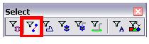
Figure 11 - Select Toolbar

  1. Right-click on any of the traces you have so far defined on you board.
  2. In the context menu that appears select Select All
  3. Right-click once more on the selected traces and select Lock
  4. All the traces you have routed will become highlighted in orange (figure 12).

6880 figure 12

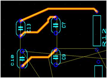
Figure 12 - Locked Traces

These copper routes are now locked and therefore cannot be altered by the autorouting process that you are about to apply to your design.

We are now ready to begin autorouting:

  1. Select Autoroute > Start/Resume Autorouter
  2. NI Ultiboard will route the rest of your copper on your board (on this board this should take a matter of seconds and will look similar to Figure 13).

6880 figure 13

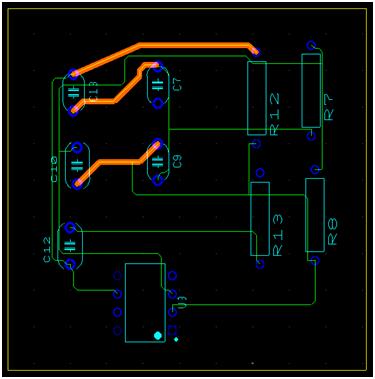
Figure 13 - Completed Routed Board

Back to Top

8.  Best Practices: Maximizing the Use of Your Routing Methods

As discussed throughout this article we have a number of tools which allow us to effectively route our board. The autorouter should not be considered as the only routing option. In fact it is suggested that if one is to begin defining a board, you follow a procedure such as the following:

  1. Consider a component of high importance with a trace routing that can be considered critical.
  2. Route the nets for this critical component using either manual or follow-me routing
  3. Find components such as connectors or FPGA components which require routing beneath/between multiple surface mount pins.
  4. Route the nets for this component using either manual trace placement  (or follow-me routing if convenient/possible)
  5. Lock all nets in the design that have been routed using steps 1 to 4 above.
  6. Use a combination of the autorouter or connection machine to route the rest of your board.

Using this simple methodology, you can be comfortable in knowing that you can maximize the use of your time in the layout and routing stages of your design.

Back to Top

0 answers47 viewsPosted 4 months agoby Chris Bertrand
Was this helpful?
Loading...
0

Complete Ultiboard Tutorial From Start To Finish

Copied directly from National Instruments: https://knowledge.ni.com/KnowledgeArticleDetails?id=kA03q000000YH7qCAG&l=en-US   This tutorial outlines how to create a custom Ultiboard landpattern for layout. This landpattern is created…
 

This tutorial outlines how to create a custom Ultiboard landpattern for layout. This landpattern is created manually so as to precisely define the shape, size, and dimensions of a Surface Mount Device (SMD). The article will outline the steps to create a custom 20-pin SMD landpattern that can be associated with the custom component created in the Creating a Custom Component in NI Multisim tutorial.

Steps in the creation process include:

  • Creating a database group
  • Defining a custom PCB part
  • Setting the environment grid spacing
  • Placing SMD landpattern pads
  • Setting the Reference ID and Value
  • Using the Ruler Bars for Object Positioning
  • Defining the IC Package
  • Creating the 3D Model
  • Saving the landpattern to the Ultiboard and Multisim database
  • Associating a landpattern with a Multisim symbol

Please note: The landpattern you are creating in this tutorial is not a commercial package. The pad and package dimensions and spacing are used primarily to showcase an effective design procedure in Ultiboard.

The term landpattern and footprint will be used interchangeably throughout this tutorial.


Create a Database Group

Ultiboard and Multisim both share a common database structure which organizes the various components into logical groups. The creation task therefore begins in the Ultiboard Database Manager.

  1. Select Tools >> Database >> Database Manager to display the Database Manager (Figure 1).

Figure 1   Database Manager

Figure 1 - Database Manager

  1.  In the Database Manager select the User Database (the red square in Figure 1 above).
Custom groups can be created in the Database Manager to logically organize where to save the footprint. The database group does not have to be created for every new component. The groups are created to assist in organizing the database appropriately. If a group has already been created which your custom component can be saved to, you can skip directly to e.
  1.  Select the New Database Group icon (the yellow square in Figure 1 above).
  2. A new branch will appear to signify a group in the User Database root. Enter the group name, Custom SMD.
  3. Select the Create a new part icon (the blue square in Figure 1 above).  NI Ultiboard will display a dialog box displaying the options of the type of component to create as displayed in Figure 2.

Figure 2   Select Part

Figure 2 - Select Part

  1.  Select the PCB part option in the dialog box shown in figure 2.

The Ultiboard design area will now be in the ‘Footprint edit mode’ and display the x?? symbol (Figure 3). x? represents the Reference Designator (RefDes) and ? represents the Value of the component. These values will be edited later in the design process in Step 4.

Figure 3   Footprint Edit Mode

Figure 3 - Footprint Edit Mode

Edit the Grid Spacing

It is important to begin the design process by setting the units of measurements for the landpattern design grid. When placing components, the design grid is what objects will snap to when they are being moved and/or placed. The grid spacing therefore defines the degree of precision with which objects can be placed in the work-area.

  1. Select Options >> PCB Properties.
  2. Click on the Grid & Units tab.

Figure 4   Grid Properties

Figure 4 - Grid Properties

  1. In the units section (Figure 4) set the Design Units as mil.
  2. To set the various Ultiboard design grids select Component Grid in the Grid Step Name combo box (the red box in Figure 4).
  3. Set the Grid Step Value to 1 mil
  4. Select the Copper Grid in the Grid Step Name combo box.
  5. Set the Grid Step Value to 1 mil

With these settings both components and copper will be placed on a 1 mil by 1 mil design grid.

Placing Landpattern Pins

Both THT (through-hole technology) pins and SMD (surface mount device) pads can be placed onto a custom landpattern. The following steps will outline how to add an array of SMD pads.

  1. Select Place >> Pins. This will display the Place Pins dialog box (Figure 5).

Figure 5   Pin Properties Dialog

Figure 5 - Pin Properties Dialog

You will now define a 10 by 2 array of SMD pins for our custom landpattern.

  1. Select the SMD Pin radio button. The following values, such as Top, Pin Length, Pin Width and Pin Radius define the shape and physical dimension of the each pin. Set the following values in Table 1 to define the pin properties (as in Figure 6);

Table 1: Pin Dimensions

Field Name

Value

Field Description

Top

Rounded Rectangle

The top field described the shape of the pad. Other options include Round, Rectangle etc…

Pin Length

58.34

The pin length defines the vertical dimension of the pin

Pin Width

15

The pin width defines the horizontal dimension of the pin

Pin Radius

7.5

In the case of rounded objects, the pin radius defines the radius of the circular part of the object

Figure 6   Set SMD Pin Properties

Figure 6 - Set SMD Pin Properties

  1. You will now create the 10 by 2 SMD pin array to place on the landpattern. The vertical and horizontal spacing that will now be set indicate the center-to-center distance between adjacent pins. Set the following spacing values in Table 2. The dialog box should look like Figure 7.
  2. Click on the OK button to place the pads onto the landpattern

Table 2: Pin Spacing

Field Name

Value

Field Description

Vertical

25

The center-to-center vertical spacing between adjacent pins.

Horizontal

200

The center-to-center horizontal spacing between adjacent pins.

Rows

10

The number of rows in the pin array

Columns

2

The number of columns in the pin array

Note: The above dialog settings can be changed to fit your specific landpattern. For example, if both Rows and Columns are set to 1, you can place individual pins.

Figure 7   Set SMD Pin Spacing

Figure 7 - Set SMD Pin Spacing

Pin 1 of the pin array is the upper-left pad and is attached to the mouse cursor.   To accurately place the pad so that the reference point is in the middle of the pad press the asterisk key (*) on the right number pad (not shift + 8). Laptop users must press FN + 0.

The Ultiboard work area will now appear as in Figure 8. You will notice that our pins are oriented incorrectly (vertically, rather than horizontally) and must be rotated by 90 degrees.

Figure 8   Pin Setup

Figure 8 - Pin Setup

  1. In the Select toolbar, click the Enable Selecting SMD pads icon as shown in Figure 9.

Figure 9   Select Toolbox (SMD Pads)

Figure 9 - Select Toolbox (SMD Pads)

  1. Drag the mouse across the design area to create a selection box, which selects all of the SMD pins
  2. Double-click on one of the selected pins. The SMT Pin Properties dialog box will appear. Select the General tab.
  3. Select the Angle (degrees) combo box and set to 90 degrees (as in the red box in Figure 10). Click on the OK button to save the change. You will notice that the SMD pins have been rotated and now look like Figure 11

Figure 10   Pin Angle

Figure 10 - Pin Angle

Figure 11   Final SMD Pin Orientation

Figure 11 - Final SMD Pin Orientation

Changing Pin Names and Values

During the creation of a new landpattern pins may be placed onto the design in a random order. It may therefore become necessary to edit the value associated with each pin so that they are numbered sequentially around a package.

  1. In the Select toolbar, click the Enable Selecting SMD pads icon as shown in Figure 9.
  2. Double-click on the pin in the bottom right-hand corner. The SMT Pin Properties dialog will appear. Select the Attribute tab.
  3. The attribute list (Figure 12) displays the tag which stores the pin number (NUMBER), the pin value (20) and its visibility (None).
  4. Select the NUMBER tag in the attribute list, which will activate the Change button (red box in Figure 12). Click the Change button.

Figure 12   SMD Pin Properties

Figure 12 - SMD Pin Properties

  1. In the attribute dialog box, changing the Value field (red box in Figure 13) will change the value of the pin.

Figure 13   SMD Pin Attributes

Figure 13 - SMD Pin Attributes

In general a package such as this has the pins numbered sequentially in a counter-clockwise direction. Therefore pin 10 should be in the bottom left-hand corner and pin 11 in the bottom right-hand corner. The final pin number configuration for this design should be as in Figure 14. Therefore to change the pin number;

  1. Change the Value field to 11 and click on the OK button. Click on the OK button in the SMT Pin Properties dialog box to save the changes.
  2. Repeat 4., 5. and 6. for all the pins for the required configuration (as in Figure 14).

Figure 14   Component Pin Setup Map

Figure 14 - Component Pin Setup Map

Setting Reference ID and Value location

In Figure 11 you will continue to notice the x?? symbol, which represents the Reference Designator and Value of the landpattern.

The Reference Designator is the key identifier of the component and is represented as x?. This x can be changed so that it corresponds with the type of component it is associated with. For example, if this landpattern was for a resistor this value could be set to R. The ? represents a number to denote the different components in a design. So, returning to the example of a resistor, the resistors placed onto a design, would be named R1, R2, R3 etc…

Value, represented by the ? symbol, is the physical value of the component. Taking the example of the resistor into consideration once more, the ? could equal 20k for 20 Kohms.

In this step you will select, move and alter the RefDes and value.

  1. In the Select toolbox, click the Enable Selecting Attributes icon as shown in Figure 15 (in the red box). This will allow you to refine the selection of components on the landpattern to be only the RefDes and Value attributes.

Figure 15   Select Toolbox (Selecting Attributes)

Figure 15 - Select Toolbox (Selecting Attributes)

The RefDes and Value are currently overlapping the landpattern placement as shown in Figure 11.

  1. Click on the X? symbol and place it to the upper-right of the pad array.
  2. Click on the ? symbol and place it to the upper-right of the pad array.
  3. Double click on X? and select the Attribute tab
  4. In the Value field set the REFDES tag to U? as in Figure 16 (in the red box)
  5. Click on OK to apply changes.

Figure 16   REFDES Attribute Properties

Figure 16 - REFDES Attribute Properties

When the custom component is now placed the RefDes for the landpattern will be U1, U2, U3 etc…

Generally the Value attribute, ?, is set to either visible or invisible depending on the need to highlight the value of the landpattern on the final design. In this example, it will be set to invisible.

  1. Double click on X? and select the Attribute tab
  2. In the Visibility section of the attributes set the Invisible radio button

Using the Ruler Bar

Both along the top and left side of the Ultiboard design area are the ruler bars in Figure 11. If the ruler bars cannot be seen, go to View >> Ruler Bars. These ruler bars allow the positioning of dashed lines to align shapes from one object to the next, precisely within the design area. For the following steps refer to Figure 14 for the pin numbers.

  1. Left-click in the horizontal (top) ruler bar area for a small arrow marker to appear and move the marker immediately to the right of pin 1 (Figure 17).
  2. Left-click to place a marker, 5 mils to the right of the marker placed in a. You will notice that the distance between two markers is displayed in the ruler bar (Figure 17)
  3. On the vertical (left) ruler bar place another marker directly above pin 1 (Figure 17)
  4. Repeat 1., 2. and 3. to align ruler bar markers at the right and bottom of the SMD pad arrays as shown in Figure 17.

Figure 17   The Ruler Bar

Figure 17 - The Ruler Bar

These markers will now act as a guide on where to begin the placement of the landpattern shape on the silkscreen layer in step 7.

If at any time markers need to be cleared, you can right-click on a specific marker and select Clear, or select Clear All to remove all markers.

Place the Landpattern Shape on the Silkscreen

The placement of shapes on the silkscreen layer defines how the custom component will appear in your design. It represents the physical dimensions of the package. In this step you will utilize the ruler markers set up in step 4 to place a rectangular landpattern shape.

  1. In the Design Toolbox (Figure 18) double-click on the Silkscreen Top to make that particular layer active. This will highlight the layer in a red.

Figure 18   Design Toolbox

Figure 18 - Design Toolbox

  1. Select Place >> Shape >> Rectangle.
  2. Ultiboard, now in a drawing mode is prepared to draw a rectangle. Line up the mouse to the upper left hand point (5 mils from pin 1 as indicated by the ruler markers in Figure 16).
  3. Left-click and drag the mouse, drawing a rectangular shape within the inner rectangle of Figure 11.
  4. The rectangle will appear as a solid, filled-in shape. Click on the Enable selecting Other Objects icon in the Select toolbar (Figure 19) and double-click on the solid rectangle.

Figure 19   Select Toolbox (Select Other Objects)

Figure 19 - Select Toolbox (Select Other Objects)

  1. In the Rectangular Properties dialog, select the General tab. In the Area section click on the Style button to change the black rectangle to a rectangular outline as in Figure 20 (red box). Click on the OK button.

Figure 20   Rectangle Properties

Figure 20 - Rectangle Properties

The landpattern will now appear as shown in Figure 21.

Figure 21   Final Landpattern

Figure 21 - Final Landpattern

Creating a 3D Landpattern

In Ultiboard a design can be previewed in 3D to virtually represent the final design. In order to setup the custom landpattern for this 3D preview, the necessary information should be setup at the creation stage.

  1. In the Design Toolbox (Figure 18) double-click on the Silkscreen Top to make that layer active. This will highlight the layer in a red.
  2. Click on the Enable selecting Other Objects icon in the Select toolbar (Figure 19) and right-click on the rectangle package shape. Select Copy in the pop-up menu.
  3. Select Edit >> Paste and place the ghosted image onto the Ultiboard work area to the right of the landpattern.
  4. Double click on the copied rectangle and select the Position tab in the Rectangle Properties dialog box.
  5. In the Layer combo box select the 3D-info Top option as shown in Figure 22. Click on OK.

Figure 22   3D Rectangle Properties

Figure 22 - 3D Rectangle Properties

  1. You may notice that the copied 3D box has now disappeared as it becomes associated with the 3D layer, which is not currently an active layer. To view the rectangle again, double-click on the 3D-InfoTop layer in the Design Toolbox to make it active. The 3D rectangle will appear in red.
  2. Select the 3D info rectangle and move it so it is positioned directly on top of the original silkscreen shape.
  3. Double click the black work-area and select the tab for 3D data
  4. Set the properties for the 3D information (Table 3) and the dialog will appear as in Figure 23 (in the red box). Click the OK button.


Table 3: 3D Information

Field Name

Value

Field Description

Enable 3D for this object

Checked

Enables Ultiboard to render a 3D object

Height

45.27555

The height in mils of the 3D object

Offset

1.96850

The offset height from board

Use 2D data to create 3D shape

Checked

Uses the 2D shape on the silkscreen layer to create the package shape

Solid Shape

Selected

Creates a solid 3D representation


Figure 23   3D Settings

Figure 23 - 3D Settings

  1. From the 3D Data tab select the Pins section
  2. Set the properties for the 3D Pin information as in Table 4. Click on the OK button.


Table 4: 3D Pins

Field Name

Value

Field Description

Angle to Pad

90

Sets the angle at which Ultiboard will render the pin connections with respect to the package.

Pin Shape

Checked

Defines the shape of the 3D pin

Type

SMDPIN

Renders the specific type of pin

In the 3D Preview you should immediately notice that the pins on the left side of the component face away from the package. This is because by default, the leads on a horizontal SMD pin will be directed towards the left. Therefore the pins must be re-orientated towards the package by rotating them 180 degrees.

  1. In the Select toolbar, click the Enable Selecting SMD pads icon as shown in Figure 9.
  2. Hold down the CTRL key and select the right column of pins on the landpattern
  3. Double-click on one of the selected pads.
  4. In the SMT Pin Properties dialog box select the General tab

Recall, in step 3 that the pins were set to 90 degrees for a horizontal orientation.

Due to this 90 degree rotation, we must rotate an additional 180 degrees, in the above step so that the 3D leads are now directed towards the component. 90 + 180 = 270 degrees.

  1. In the Angle(degrees) combo-box set the angle to 270.
  2. Click on the OK button.

If you double click in the black work-area and select the tab for 3D data you will notice that as in Figure 24, the pins are properly positioned with respect to the 3D package.

Figure 24   3D Pin Settings

Figure 24 - 3D Pin Settings

Saving the Landpattern

With the landpattern created all that remains is saving the to the Ultiboard database.

  1. Select File >> Save to Database.
  2. In the database section select the Custom SMD group created in step 1 (Blue box in Figure 25).
  3. Name the component SMD20 as in Figure 20 (red box).
  4. Click on the OK button.

Figure 25   Save Dialog Box

Figure 25 - Save Dialog Box

Adding the Landpattern to a Multisim Database

Before a custom landpattern can be utilized in Multisim, it must be added to the database. Once added to the database, it can be seen as an available landpattern, or footprint, and added to a component.

In this step, the SMD20 tutorial landpattern created will be associated with the symbol created in Part 1 of the tutorial.

  1. Open NI Multisim.
  2. Select Tools >> Database >> Database Manager.
  3. In the Database Manager select the Components   tab. Under the Database Name, select the User Database.
  4. In the Component List select the THS7001 component and click on the Edit button.
  5. In the Component Properties dialog box click on the Footprint tab.
  6. Click on the Add from Database button.
  7. In the Select a Footprint dialog box select the User Database (red box in Figure 22). You will notice that currently the User Database does not see the landpattern that has been created in Steps 1 to 9 of this tutorial.
  8. To add the landpattern click on the Add button (blue box in Figure 26).

Figure 26   Multisim Database Manager

Figure 26 - Multisim Database Manager

  1. In the Add a Footprint dialog box set the following data as shown Table 5. The dialog box will appear as in Figure 27 (red box);

Table 5: Add a Footprint

Field Name

Value

Field Description

Database Name

User Database

The database in which you saved the landpattern in Ultiboard

Manufacturer

Generic

An additional manufacturer identifier

Footprint

SMD20

This is a CASE SENSITIVE field, and must identify the landpattern exactly as it is saved in Ultiboard

Ultiboard Footprint

SMD20

This is a CASE SENSITIVE field. While the Footprint field identifies the specific package name of the component it can be associated with the Ultiboard Footprint so that a generic footprint with the same dimensions can be transferred to layout

Number of Pins

20

Number of pins on the landpattern

SMT/TH

SMT

The type of pin technology Surface Mount or Through Hole

Figure 27   Add a Footprint

Figure 27 - Add a Footprint

  1. Click on the OK button.
  2. You will notice that the SMD20 can now be previewed within the dialog box. Click on the Select button to select the newly added SMD.
  3. Click on the OK button to save the component settings.
  4. Save the component to the appropriate database and group (as it was originally saved to) and click on the OK button. You will be prompted to overwrite the original component. Choose the Yes button.

Success!! You have created a custom Ultiboard landpattern, defined a 3D model and associated it to a Multisim symbol.

0 answers55 viewsPosted 4 months agoby Chris Bertrand
Was this helpful?
Loading...
0

Search Site

K.C.D. 2024+ Site Stats

  • Users 654
  • Articles 3